X-ray Optics...Optics for XEUS
Novel Technologies for Future Large X-ray Telescopes
Shaping of Advanced Si wafer X-ray Optics
R. Hudec,
,
L. Pína,
A. Inneman, V. Semencová, M. Skulinová, L. véda, V. Broek, J. ik, M. Míka, R. Kačerovský, T. Kubina,
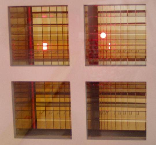
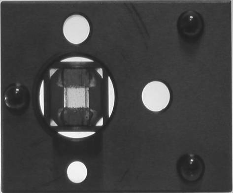
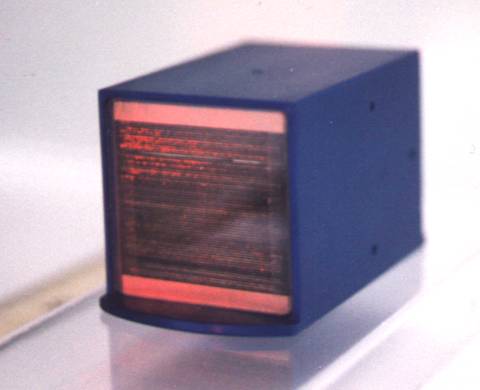
X-ray Multi Foil Optics (MFO)
X-ray optics based on multiple thin X-ray reflecting foils
The foils may be of various materials (e.g. glass, Si, metals)
Various arrangements and geometries possible, e.g. LOBSTER, K-B, Wolter, double conical approximation to Wolter, etc.
Various examples of X-ray MFO: foil thicknesses from 30 microns to 1 mm, foils 3 x 3 mm to 300 x 300 mm, planar & ellipsoidal
Our approach to X-ray MFO based on Si wafers
the Si wafers parameters are optimised already at the production stage
the Si wafers are shaped to precise optical surfaces/shapes
the internal stress is minimised
the shaped/bent Si wafers are stacked to form the MFO
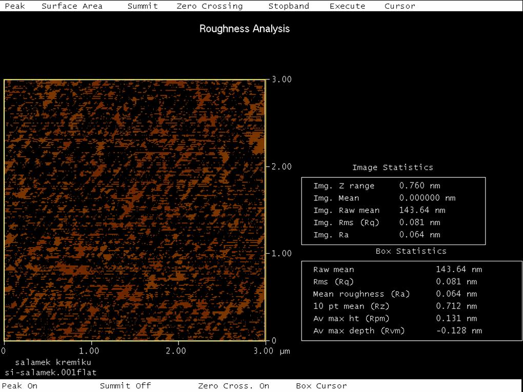
MEASURING THE QUALITY OF SI WAFERS
the production of Si wafers is a complex process
at moment, the production of Si wafers is NOT optimised for X-ray optics applications
precise measurements and optimization already at production stage are important for X-ray optics based on Si wafers
Example of specification of standard Si wafers,
individual parameters may be improved according to customer requirements.
Optical profilometer STIL
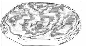
Thickness homogenity of Si wafer produced by ON Semiconductor Czech Republic
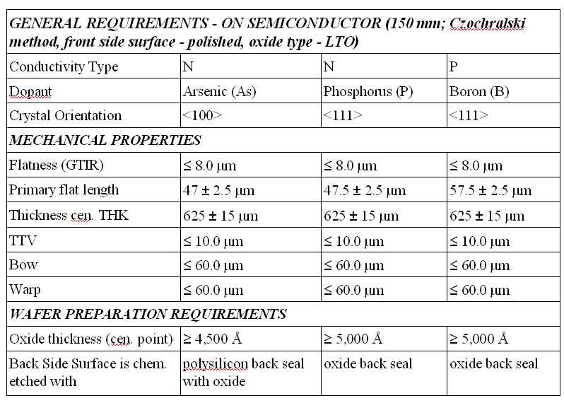
Flatness and thickness uniformity of a Si wafer (diameter 150 mm)
Flat Si wafer, diameter 150 mm ON Semiconductor Czech Republic, profilometer measurement, 2 perpendicular axes
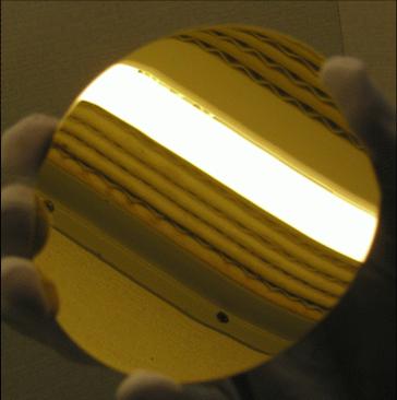
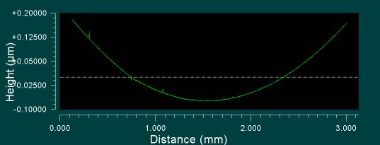
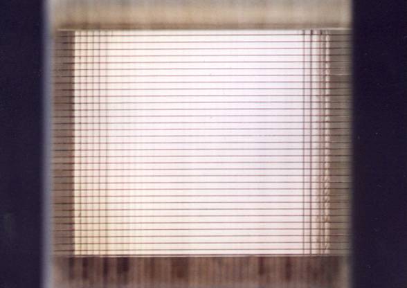
100 mm diameter, 0.8 mm thick Si wafer before (left) and after (right) bending (test cylinder R = 1.3 m)
Si WAFERS SHAPING . test cylindrical samples.gold-coated, d=100 mm, thickness 0.8 mm, R=1.3 m
DEVIATION / bent Si wafers
before processing (deviation from plane)
after processing (deviation from cylinder)
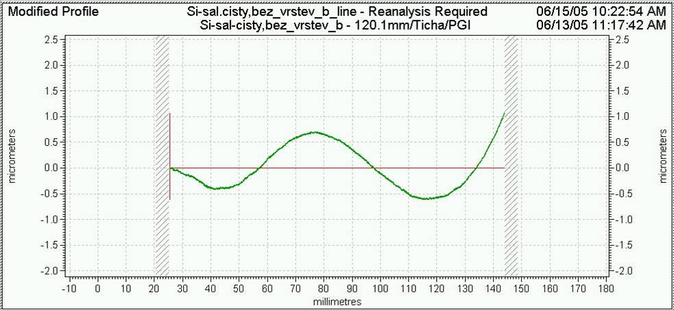
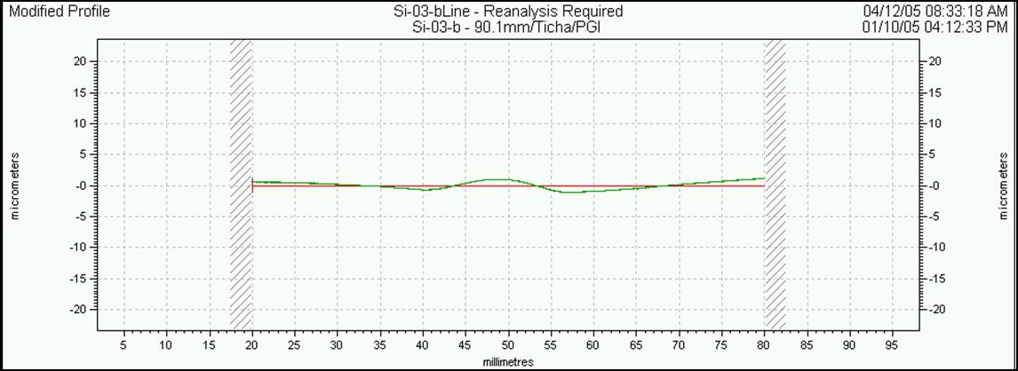
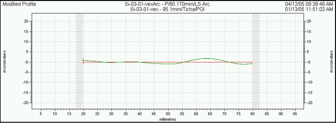
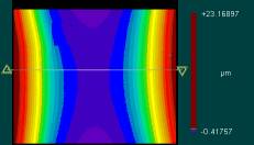
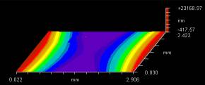
Parabolized Si wafer, D=100 mm
Interferometer ZYGO
profile plot
3D plot
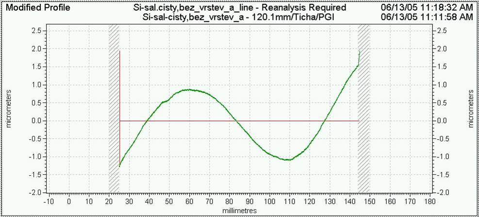
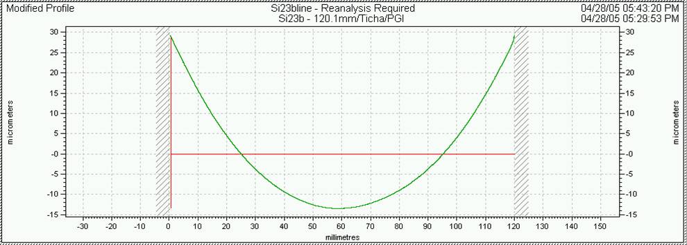
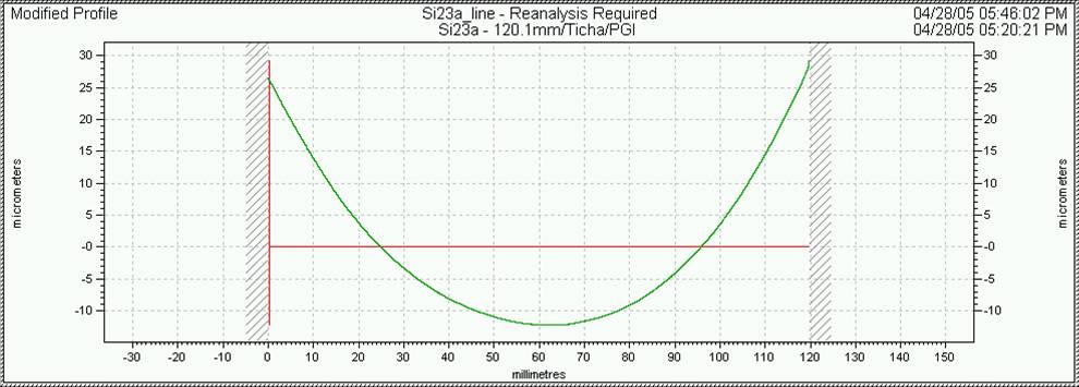
Parabolized Si wafer, sample 2, D=150 mm,
ON Semiconductor profile measurement in 2 perpedicular axes
before processing (deviation from plane)
after processing (deviation from cylinder)
Summary - Si wafers
Interdisciplinary co-operation (team with 10 members) created within the Czech Republic with experienced teams including researchers at the large company producing Si wafers
Si wafers succesfully bent to desired geometry by 2 different techniques, the 3rd technique will be tested within 1 month
The bending before stacking is advantageous eg. to avoid increase of internal stress and to allow very long-term stability of the mirror array
The production of Si wafers very complex, need to modify and optimize the parameters at the production stage
Need to minimize the internal stress (25 years lifetime...)
The production of Si wafers and related techniques carefully analysed
MLs succesfully deposited and tested
Next steps:
3rd bending technology
bending of larger and high quality Si wafers
measurements of internal stress
tests of stacking
better measurements, metrology
tests at production stage to modify the parameters, decrease stress, allow more easy bending etc
DOWNLOAD THE DOCUMENT
|
BACK
|
HOME
Basic Information
Integral Project Czech Office
Integral Project - CVs Working Group
Integral Project - Blazar Working Group
BART Robotic Telescope
BLAZARS and AGN
Wide-Field Sky Imaging
X-Ray Optics
Wide-Field Optics
Replicated X-Ray Optics
Light-weight X-Ray Optics
Optics for XEUS - 1
Optics for XEUS - 2
Home
LOBSTER Project
Gamma-Ray Bursts
Observation Network
Image Galery
Links
Page generated:
-->